-
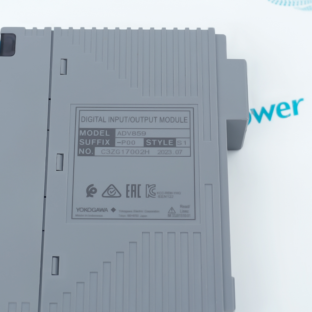
Match the complete marking
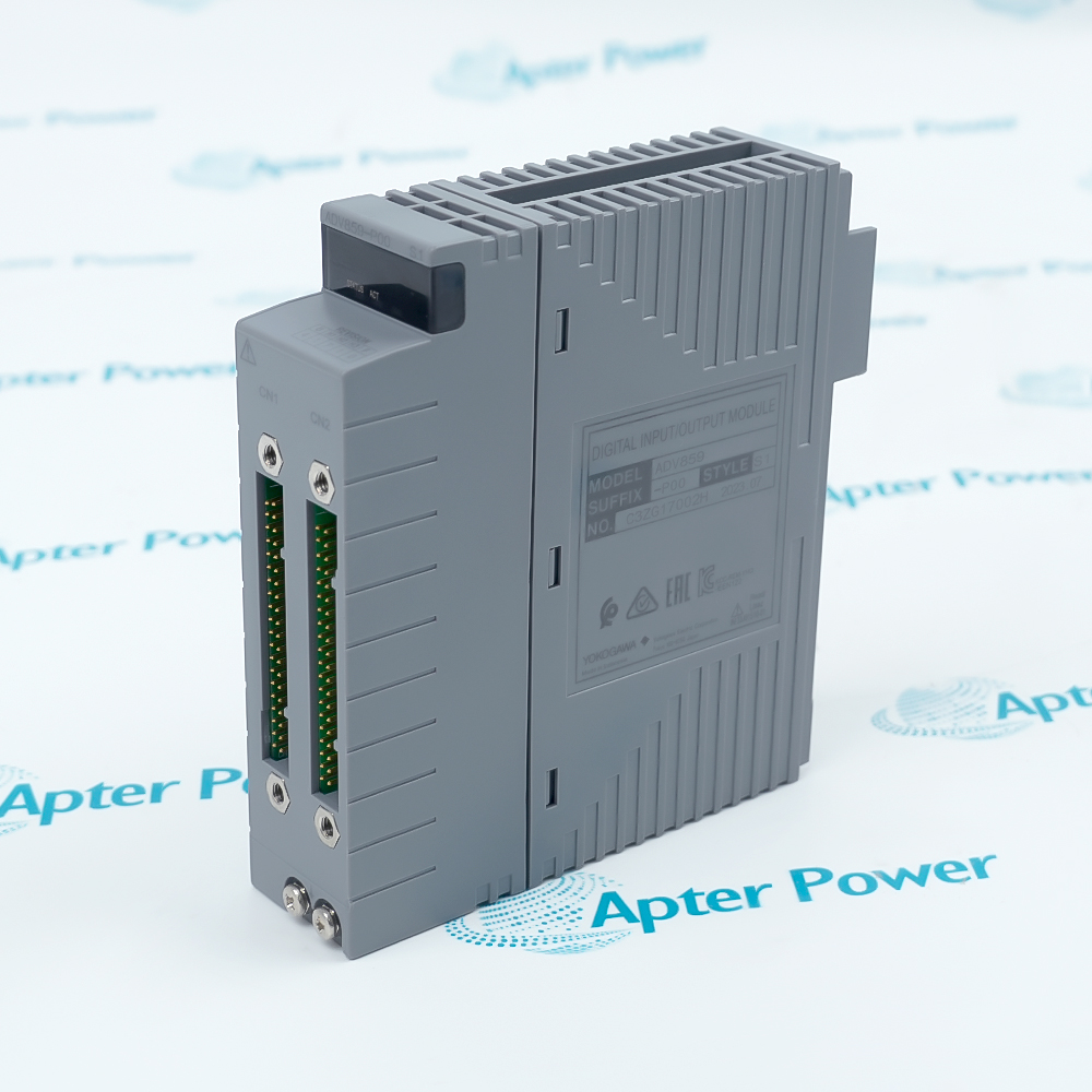
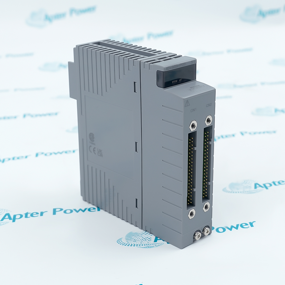
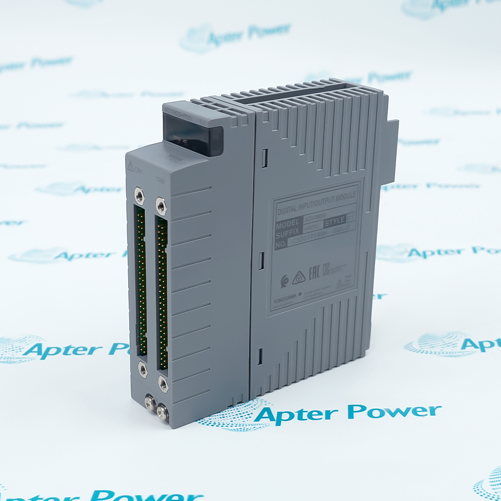
Include the complete Yokogawa ADV859-P00 S1 marking and any revision or assembly number visible on the item. Preserve the ST2 field interface and KS2 cable identity.
-
Check the offered item before ordering
Request available label and connector photos. Have your maintenance team compare the offered ADV859-P00 S1 with the installed equipment and applicable Yokogawa documentation.
Technical specifications for ADV859-P00 S1
-
Manufacturer:Yokogawa
-
Product Category:DCS Systems
-
Spare Part Number:ADV859-P00 S1
-
Weight:0.2 kg
-
Tariff Code:8537101190
-
Input channels:16
-
Output channels:16
-
Channel isolation:Individually isolated channels
-
Contact ON threshold:≤200 Ω
-
Contact OFF threshold:≥100 kΩ
-
Input contact rating:≥5 VDC / 20 mA
-
Short-circuit sensing current:Minimum 1.25 mA
-
Voltage ON threshold:±1 VDC; source resistance ≤200 Ω
-
Voltage OFF threshold:4.5–25 VDC
-
Output contact rating:30 VDC / 100 mA
-
Input response:8 ms, status input
-
Output response:≤16 ms
-
Pulse width:8 ms to 7200 s
-
Pulse resolution:8 ms; additional ON/OFF delay ≤1 ms
-
5 V current consumption:Maximum 450 mA
-
Field cable:KS2
Information
- Yokogawa ADV859-P00 S1 retains field contact sensing and switched control signals when a compatible ST2 interface is used with FIO hardware. Input-state interpretation and output timing are configured separately, so the field circuit must match both sides of the module.
Isolation: Individually isolated channels
Field connection: KS2 dedicated cable; ST2 compatibility
Contact input is ON at 200 Ω or less and OFF at 100 kΩ or more. For voltage input, ON is ±1 VDC with source resistance no greater than 200 Ω, while OFF is 4.5–25 VDC. Input contacts require a rating of at least 5 VDC, 20 mA; minimum short-circuit sensing current is 1.25 mA.
Outputs are transistor contacts rated 30 VDC, 100 mA for resistive or inductive loads, with a suppression diode required for a DC relay. Input status response is 8 ms and output response is no more than 16 ms. Pulse widths extend from 8 ms to 7200 s with 8 ms resolution and an additional maximum 1 ms ON/OFF delay.
ADV859-P00 S1 Official Technical Excerpt
The original technical excerpt for Yokogawa ADV859-P00 S1 covers ST2 interface ratings, point modes and the ADV859-P00 order code. PDF · 3 pages.ADV859-P00 S1 Installation & Verification Guide
Apter Power installation and verification guide covering KS2 wiring checks, contact thresholds, load suppression and point tests. PDF · 5 pages.
Application scope: Contact status, transistor switching and timed outputs are supported functions. Preserve the configured point modes and load protection; these are not arbitrary high-speed counter inputs.
Contact-state acquisition
16 input channels acquire approved field contacts with the defined ON and OFF resistance limits.Transistor load switching
16 output channels switch DC loads within the stated voltage/current and suppression requirements.Timed actuation
Pulse-width or time-proportional configuration supplies controlled output durations within the module timing limits.ST2 field migration
The KS2 connection maintains the compatible ST2 field interface while the module operates in the supported FIO system.
Preserve the ST2 interface and KS2 cable assignment; do not swap another ST-compatible module by appearance.
Compare actual contact resistance and leakage with the 200 Ω ON and 100 kΩ OFF thresholds.
Keep the individually isolated channels arrangement consistent with the original field circuit.
Fit the required suppression diode and observe output polarity and 30 VDC / 100 mA ratings.
Check status, pulse-width and time-proportional output assignments after configuration changes.
Exercise each affected input and output while the process is in an approved test state.
Alternative Names
Technical notes
Engineering relationship: Individually isolated channels determines how field references may be grouped. Preserve the installed KS2 cable and terminal-board circuit; a similar connector does not establish compatibility.
Installation boundary: The voltage-input ON condition is near zero volts, not a conventional positive 24 V ON threshold. Verify contact polarity and source resistance before proving the field state.
Technical basis: Yokogawa Digital I/O Modules (for FIO), GS 33J60F70-01EN, 5th edition. The ADV859-P00 base hardware ratings apply to the offered ADV859-P00 S1; retain the S1 hardware style and verify its installed FIO configuration. Other module columns are excluded.

FAQ View All FAQ
-
How does ADV859-P00 S1 keep separate field circuits electrically distinct?Its input and output channels are individually isolated. Preserve that channel separation at the ST2 terminal assembly rather than adding an unintended common return.
-
Can the KS9 cable used for ST5 replace the KS2 connection on ADV859-P00 S1?No interchangeable connection is established. ADV859 uses the dedicated KS2 cable and the ST2-compatible field interface; the cable and terminal mapping must match that arrangement.
-
What minimum contact rating is required at the inputs of ADV859-P00 S1?The field input contacts must be rated for at least 5 VDC and 20 mA. Contact suitability must also satisfy the low resistance needed for a dependable ON state.
-
Why can a leaky open contact remain ambiguous on ADV859-P00 S1?An OFF contact must present at least 100 kΩ, while ON requires no more than 200 Ω. Intermediate resistance is outside the defined contact-state thresholds and should be investigated.
-
Is an 8 ms output pulse from ADV859-P00 S1 the same as an 8 ms input response?No. Eight milliseconds is both the minimum programmable pulse width and the status-input response figure, but they describe different functions. Output response is specified separately at 16 ms or less.
-
What does the -P selection add to ADV859-P00 S1?It enables pulse-width and time-proportional output functions in addition to the module hardware role. It does not add pushbutton input capability to ADV859.
-
Can ADV859-P00 S1 switch a 200 mA actuator directly?The output contact rating is 100 mA at 30 VDC, so a 200 mA load exceeds that rating. Use an engineered interface suitable for the actual load instead of overloading the module.
-
How should ADV859-P00 S1 be budgeted on the 5 V backplane?Its maximum consumption is 450 mA at 5 VDC. Keep this figure separate from the current drawn by externally powered output loads.
Supporting new and legacy automation
-
Please try to be as accurate as possible with your search.
-
We can quote you on 1000s of specialist parts, even if they are not listed on our website.
-
We can't find any results for “”.
You May Also Like
Product Browsing History
-
Whatsapp: +86 18030235313
Send us a message. -
sales13@apterpower.com
Complete our online form. -
+86 18030235313
Speak to our team in your native language.